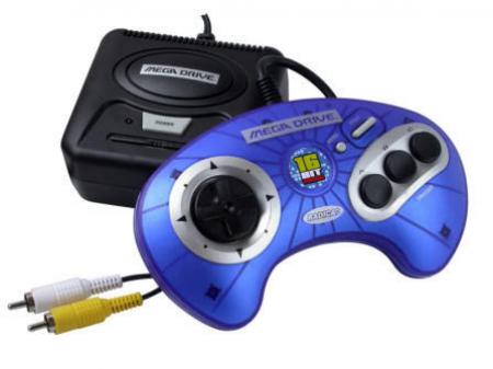
Video game consoles nowadays are powerful machines, capable of running graphically demanding games like Red Dead Redemption 2, Halo Infinite and Metro Exodus. They are indeed a Far Cry from the video game consoles in my childhood - I remember spending a better part of many weekends playing Golden Axe on the Radica SEGA Genesis 6 in 1 Vol. 1 (what a mouthful!):
Or the SpongeBob SquarePants Fry Cook Games Plug and Play console:

If we look even further back, the first video game console, dubbed “ The Brown Box”, was invented in 1967 by Ralph Baer. It was a multi-game system that included games like ping-pong and checkers. Here’s a fascinating video by the Smithsonian about the world’s first video game console.
Ever since I’ve started gaming in my pre-teens, I’ve always wondered how video game consoles were constructed, how they accepted various inputs and produced various outputs (sound, video). Fortunately, in the second part of the EdX course created by UT Austin professors Jonathan Valvano and Ramesh Yerraballi, we get to build our own video game console! Through this project, we can showcase various important microcontroller concepts: interrupts, DACs, ADCs and graphics. We will be creating a video game console for Atari’s Space Invaders!
1 Components of a Video Game Console
A video game console is like most other computer systems, where it accepts inputs, processes them and produces some output. In general, it accepts two kinds of inputs, button clicks and analog control. It then computes and changes the game state according to the inputs. Finally, it produces sound and graphics reflecting the game state.
Microcontroller concepts underlie such a system: accepting analog control uses an analog-to-digital converter (ADC), while producing sound requires the use of digital-to-analog converters (DAC) and periodic interrupts. Interrupts are also essential for updating the game state at regular intervals. Let us first explore each of these concepts.
1.1 Analog-to-Digital Converter
The world we live in is inherently analog. Physical quantities are continuously variable. Time flows continously as an infinite sequence of moments. On the other hand, computers are digital, representing information using bits such that information must be discrete. As such, how do we reconcile the digital computer with our analog world? We accomplish this digitization through two methods: discretisation (amplitude quantization) and sampling (time quantization).
1.1.1 Discretisation
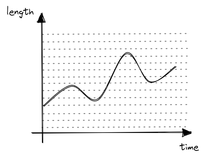
In our analog world, physical quantities are continuously variable - this means that there are an infinite number of values between any two values. For example, if we are measuring length, there are an infinite number of values between 0cm and 3cm. However, because computers are digital in nature, they cannot represent an infinite number of values given a fixed number of bits.
As such, we split the continuous range of values of the physical quantity into a finite set of “levels”. For example, instead of an infinite number of values in \([0, 1]\) cm, we discretize it into \(\{0.0, 0.33, 0.67, 1.0\}\) cm. This allows computers to represent analog values using digital bits.
However, one thing you might notice is that digital bits are not able to 100% represent analog values precisely. For example, if the analog value is 0.598cm, it will be rounded off and stored as 0.67cm in digital bits. Here, let us introduce the idea of precision and resolution. Precision is the number of “levels” while resolution is the smallest change that can be represented. If we discretize \([0, 1]\) cm into \(\{0.0, 0.33, 0.67, 1.0\}\) cm, we only need 2 bits to represent these 4 values (00 -> 0.0, 01 -> 0.33, 10 -> 0.67, 11 -> 1.0). In this case, the precision is 4 since there are 4 “levels”, while the resolution is 0.33cm as this is the smallest change possible.
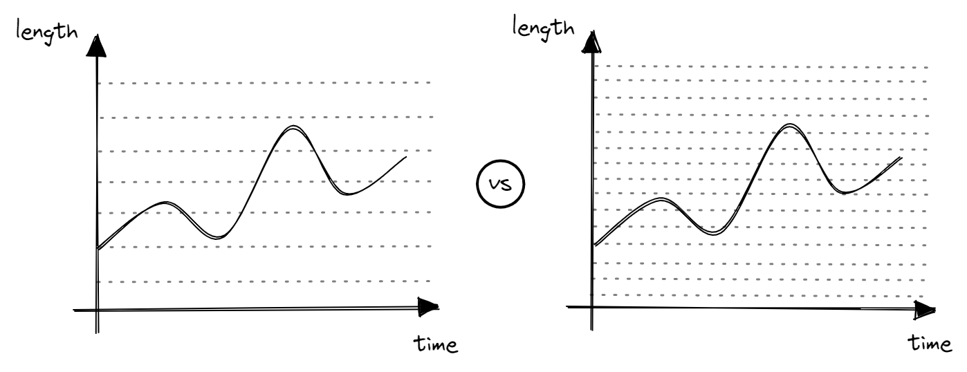
If we use 3 bits, we can represent \(2^3=8\) values. This allows us to discretize \([0, 1]\) cm into \(\{0.0, 0.14, 0.29, 0.43, 0.57, 0.71, 0.86, 1.0\}\) cm. The precision is 8 while resolution is 0.14cm. We are able to more accurately represent an analog value of 0.598cm as 0.57cm using 3 bits. As such, the more bits the computer uses to represent an analog value, the more accurate the digital representation of the analog value is. However, this increases the memory cost of representing each analog value.
1.1.2 Sampling
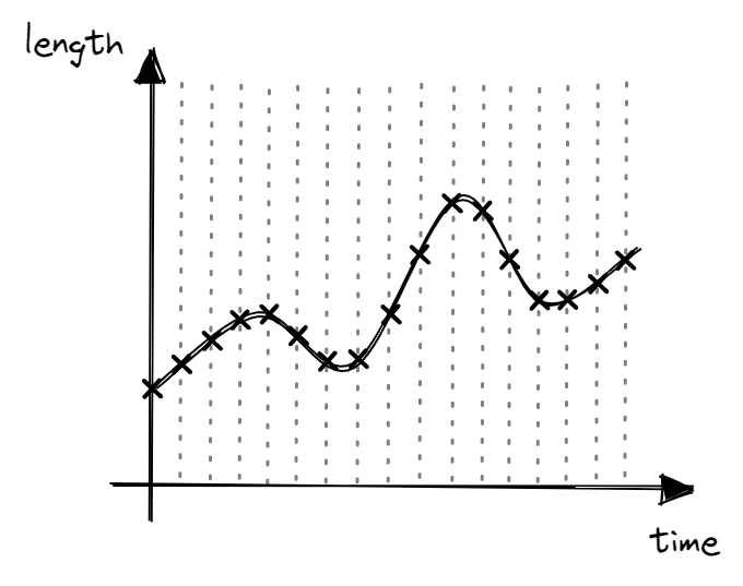
Just like physical quantities, time can also be thought of as a continuous variable. Between any two points in time there are an infinite number of moments in time. Given a fixed amount of memory, it is impossible for a computer to record measurements for an infinite number of moments in time. As such, computers sample measurements at some rate.
However, similar to discretization, you might realize that the sampled measurements will not 100% accurately represent the analog values across a time period. Intuitively, the faster the sampling rate, the more faithful the digital representation is with regards to the analog signal. Note that increasing the sampling rate comes at a cost of more processing per unit time.
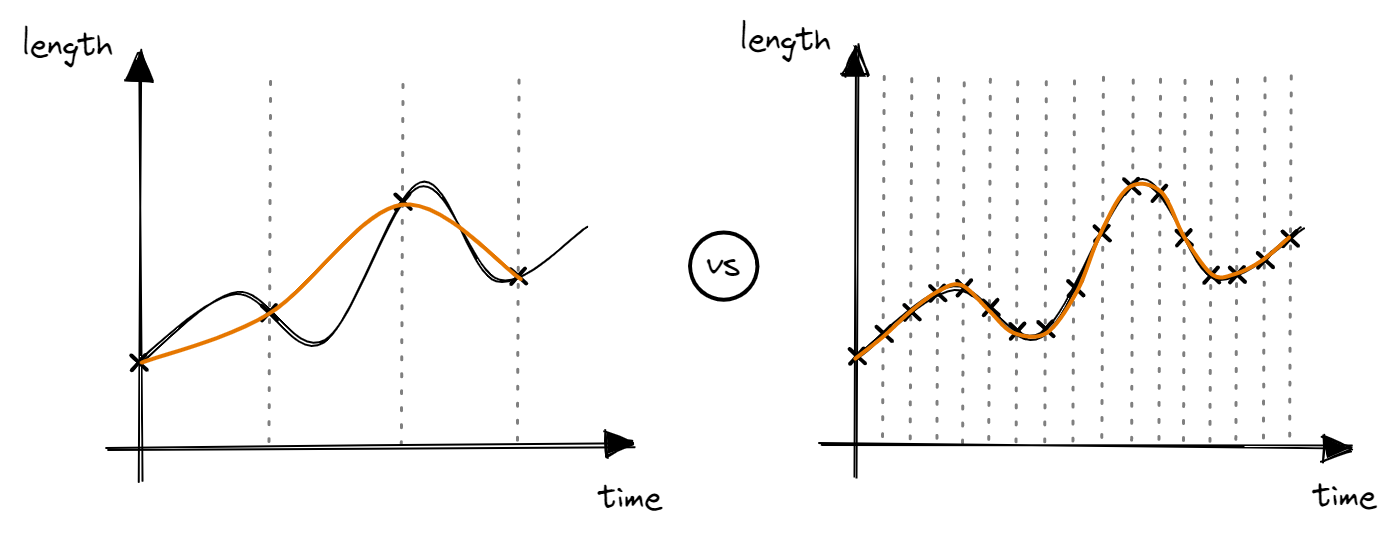
In particular, the Nyquist Theorem states that the sampling rate should be more than double the maximum frequency in order to prevent aliasiang. Aliasing is where a high frequency signal appears as low frequency due to a too low sampling rate.
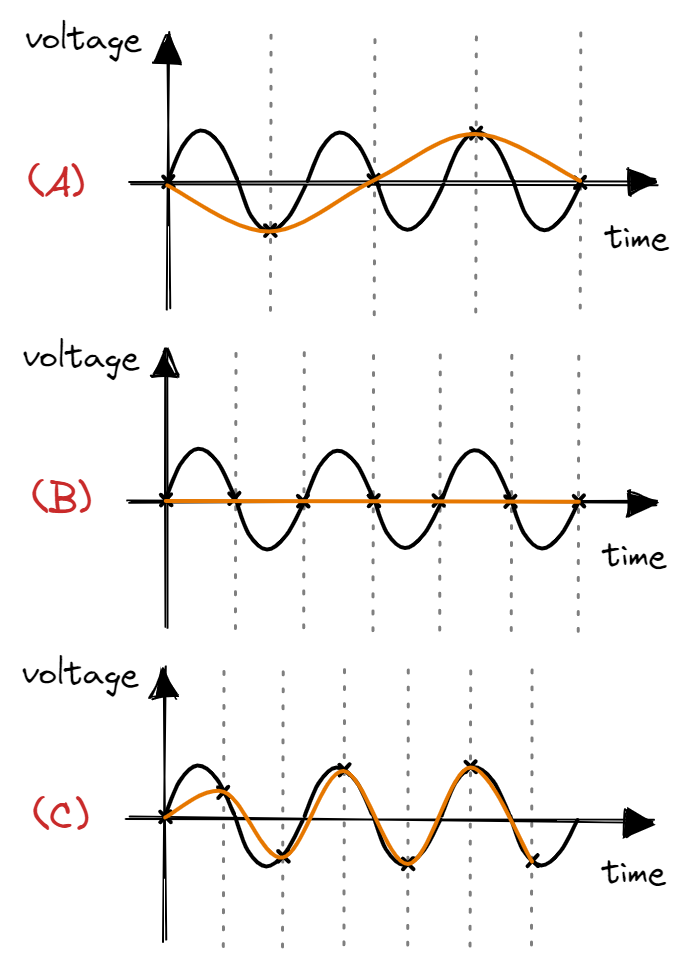
As seen above, when sampling at <=2f, the reconstructed wave will have a lower frequency compared to the analog signal. Thus, in theory, we need to sample at a rate more than double of the maximum frequency of the analog signal. In practice, we should sample at a rate significantly higher than the maximum frequency (Professor Valvano postulates that we should sample at >10f).
1.1.3 Creating the ADC
We use the concepts of discretisation and sampling in creating the ADC. On the EK-TM4C123GXL, the ADC takes in an analog signal of 0.0 to 3.3V and converts it to a digital number (0 to 4095). This means that the ADC uses 12 bits (\(2^{12} = 4096\)) - its precision is 4096 while the resolution is \(3.3V/4095 \approx 0.81mV\).
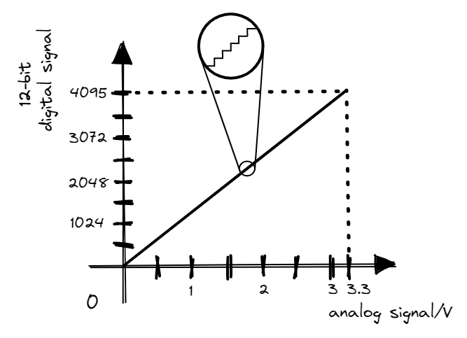
How does the ADC perform this discretisation conversion? The most pervasive method is successive approximation. But first, before we delve into what successive approximation is, let’s play a game: You’re going to think of a 8-bit number between 0 and 255, and I’m going to guess it. For each guess, you’ll tell me whether your number is either lower (<) or greater than or equal to (>=) my guess.
The most straightforward but inefficient method would be to guess each number between 0 and 255 (time complexity of \(O(N)\)). A far more efficient method would be to do a binary search (time complexity of \(O(log(N))\)). For example, assume that you are thinking of 57. I will first guess 128, in which you’ll tell me that your number is lower. Knowing that your number is between 0 and 127, I will guess 64. Again, you’ll tell me that your number is lower and I’ll know that your number is between 0 and 63. Next, I’ll guess 32 and you’ll tell me that your number is greater than or equal to 32. Deducing that your number is between 32 and 63, I will guess 48. This continues until I have successfully guessed your number of 57.
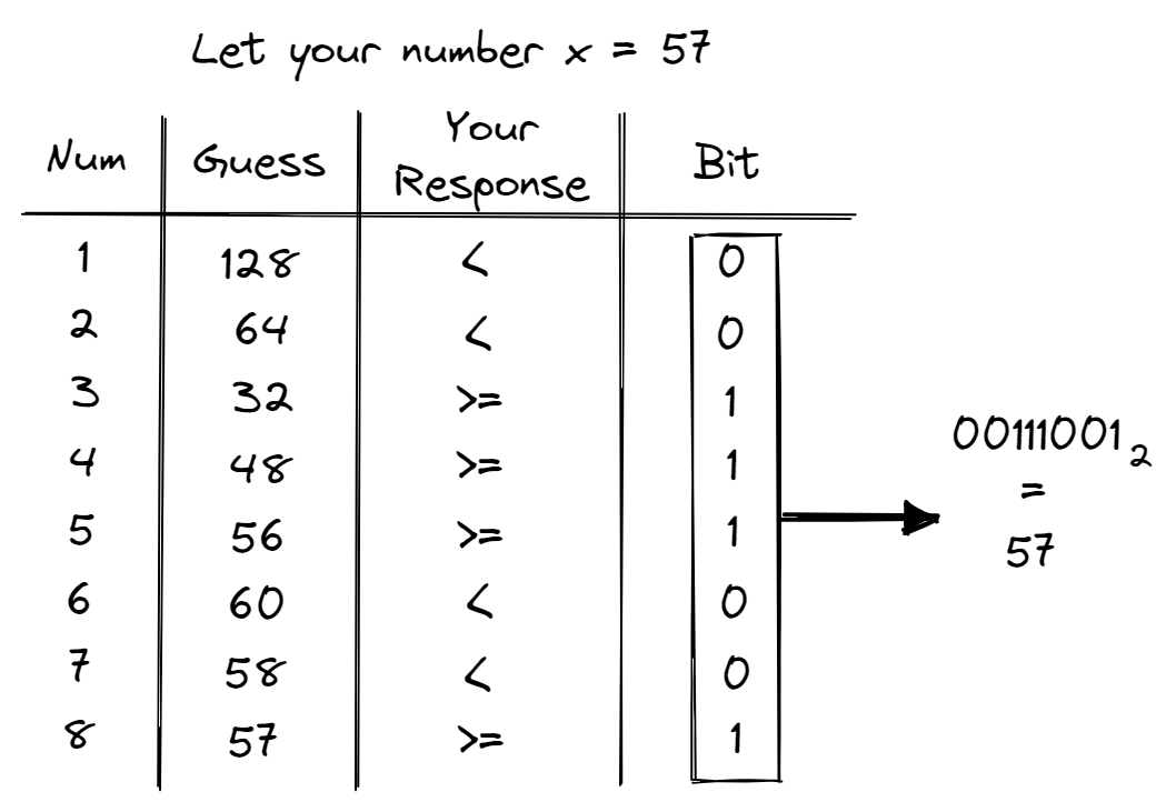
What you’ll notice is that each guess and response determines one of the 8 bits. In particular, we start with the most significant bit and work our way down to the least significant bit. This is in essence what successive approximation is - a game of guessing using binary search!
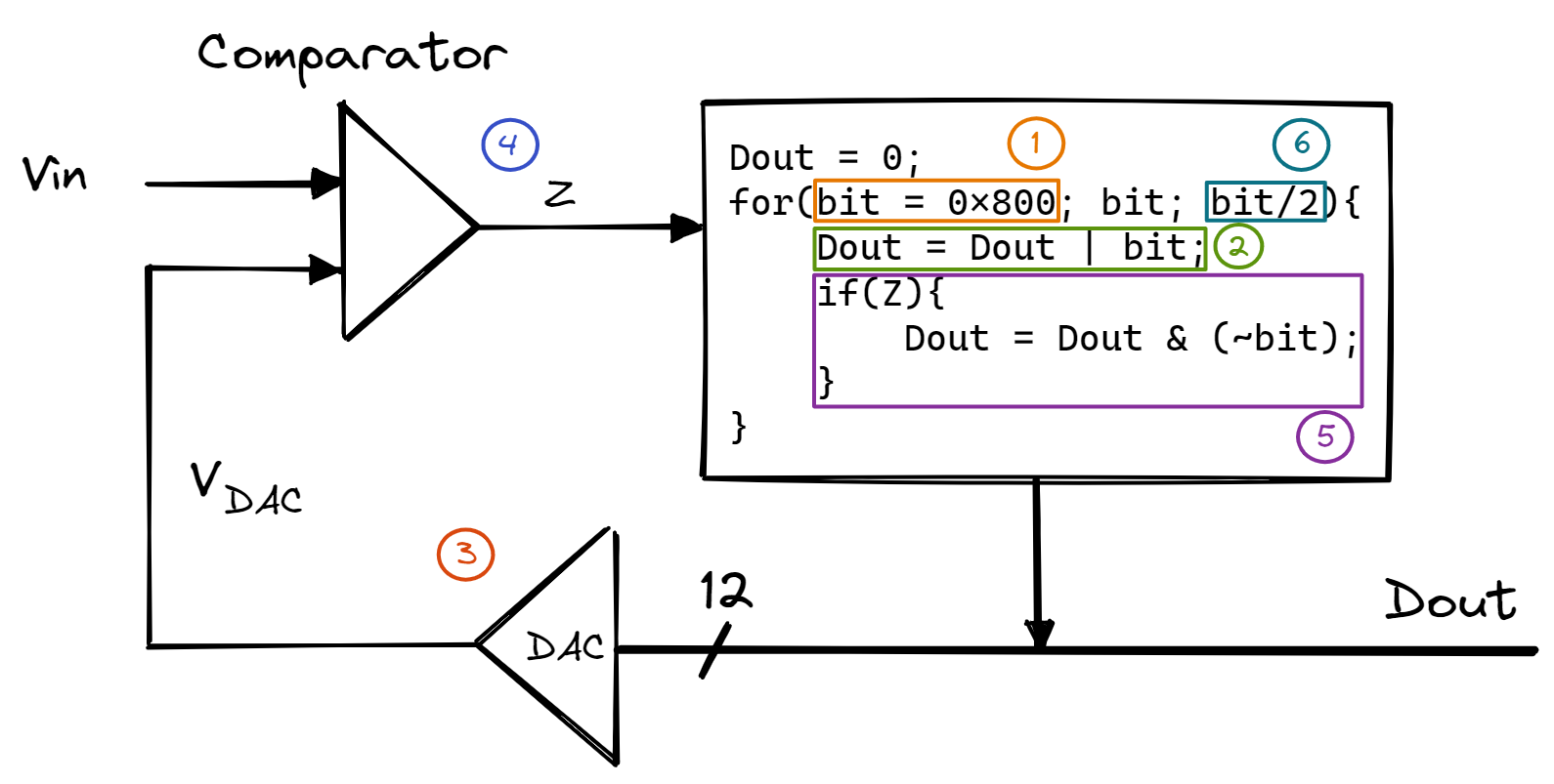
In the flowchart above, a 12-bit successive approximation ADC is clocked 12 times for one sample. At each clock (each iteration of the for loop), another bit is determined, starting with the most significant bit. At the first clock,
- The hardware issues the first “guess” by setting
bit=0x800(0x800= 2048 = \(100000000000_2\)). Doutis then set toDout|bit=0x800.- This outputs
0x800, which is fed into the DAC and converted into \(V_{DAC}=2048/4095 * 3.3V\). - Through the comparator, \(Z=0\) if \(V_{in} \geq V_{DAC}\), while \(Z=1\) if \(V_{in} < V_{DAC}\).
- We return back to the
forloop: If \(Z=1\), this means that \(V_{in} < V_{DAC}\) and so the 12th bit ofD_{out}should be cleared. - For the next iteration of the
forloop, we are going to look at the 11th bit. Thus, we setbit=bit/2=0x400(0x400= 1024 = \(010000000000_2\)) as the next “guess”.
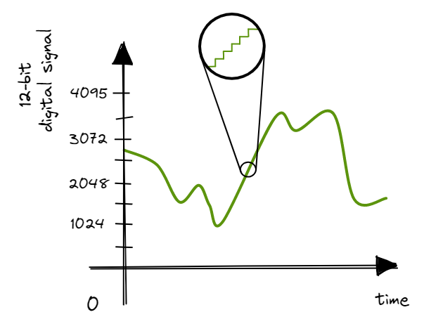
This for loop continues until all 12 bits have been determined and we have discretised the analog input voltage into a 12-bit digital number. This gives us one sample. To set the maximum sampling rate, we set bits 8 and 9 of the SYSCTL_RCGC0_R register (00 -> 125,000 samples/s, 01 -> 250,000 samples/s, 10 -> 500,000 samples/s, 11 -> 1,000,000 samples/s). The actual sampling rate will be determined by the rate at which we trigger the ADC - we’ll use periodic interrupts to trigger the ADC (we’ll explore this in section 1.3).
1.1.4 Using the ADC
How are we going to use the ADC in our video game console? We use it to read analog voltage input from a potentiometer to change the position of the player along the x-axis.
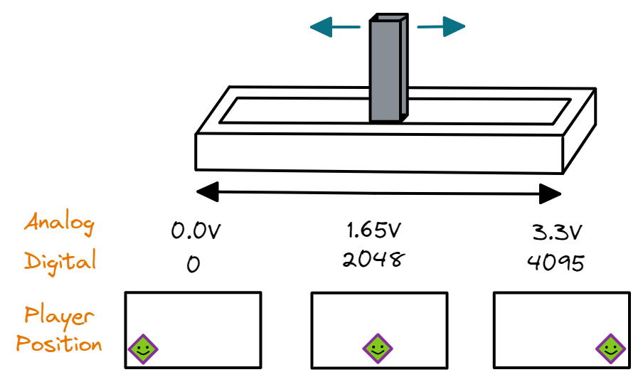
1.2 Digital-to-Analog Converter
With the digital-to-analog converter (DAC), we face a similar problem of reconciling an analog world with a digital computer, except that now we want to convert a digital number to an analog output. Given that our general purpose input/output (GPIO) pins can only be set to a low of 0.0V (digital 0) or a high of 3.3V (digital 1), how can we output a voltage that is between 0.0V and 3.3V? There are two ways to build a DAC circuit: binary weighted or R-2R ladder. Here, we will only take a look at the binary weighted circuit.
1.2.1 Binary Weighted DAC
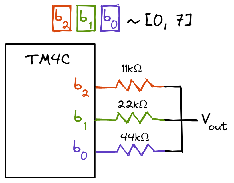
Let’s design a 3-bit binary weighted DAC that converts digital numbers between 0 and 7 to analog signals between 0.0V and 3.3V. As it has 3 bits, the precision is \(2^3=8\) while the resolution is \(3.3V/7\). Let \(b_0\) be the least significant bit and \(b_2\) be the most significant bit. To build the DAC, we connect an 11k\(\Omega\) resistor to \(b_2\)’s GPIO pin, a 22k\(\Omega\) resistor to \(b_1\)’s GPIO pin and a 44k\(\Omega\) resistor to \(b_0\)’s GPIO pin. Let’s see what happens when the DAC outputs the number 1:
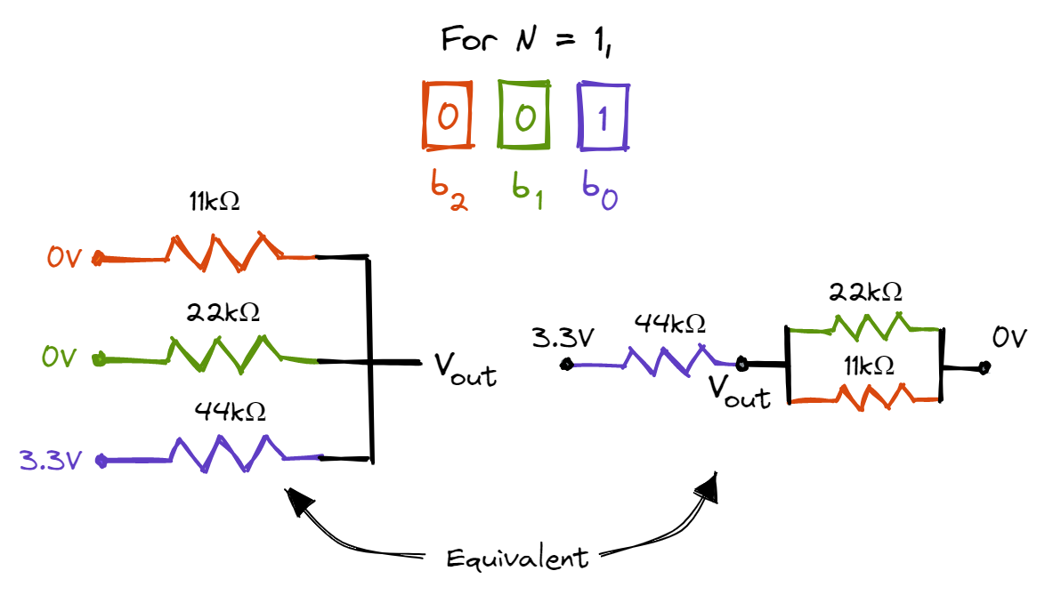
The circuit on the right is equivalent to the circuit on the left. As the 11k\(\Omega\) and 22k\(\Omega\) resistors are in parallel, the effective resistance is 22k/3\(\Omega\). As such, \(V_{out}\) = \(\frac{22/3}{44 + 22/3} * 3.3V = \frac{1}{7}*3.3V\). Next, let’s examine what happens when the DAC outputs the number 2:
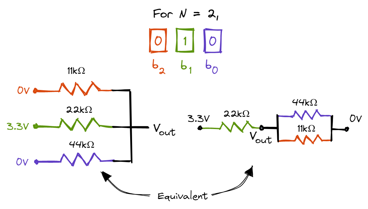
As the 11k\(\Omega\) and 44k\(\Omega\) resistors are in parallel, the effective resistance is 44k/5\(\Omega\). As such, \(V_{out}\) = \(\frac{44/5}{22 + 44/5} * 3.3V = \frac{2}{7}*3.3V\). Using the same analysis, we discover that when the DAC outputs the number 4, \(V_{out} = \frac{4}{7}*3.3V\). Utilising the Superposition Theorem, we can determine all the different outputs of the DAC:
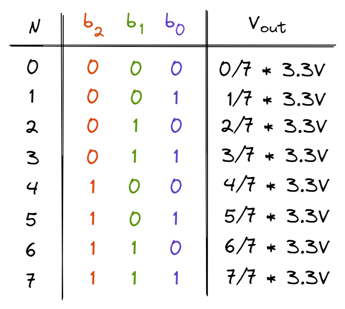
As such, using the binary weighted circuit, our DAC is now able to output voltages that are between 0.0V and 3.3V. Of course, as we increase the number of bits of our DAC, the greater the precision of our DAC. For example, a 5-bit DAC will have \(2^5=32\) levels and a resolution of \(3.3V/31\). However, one flaw of the binary weighted DAC is that the value of resistors grow exponentially. For a 5-bit DAC where the smallest resistor is 11k\(\Omega\), the largest resistor will be a whopping 176k\(\Omega\). This can be mitigated by using the other kind of DACs, R-2R ladders (which we won’t use for the sake of simplicity).
1.2.2 Using the DAC
Just like the ADC, how are we going to use the DAC in our video game console? We will be using it to produce sound! First, what is sound? Sound is a pressure wave propagating through a medium like air or water. Let’s analyse sound waves as a sinusoidal wave:
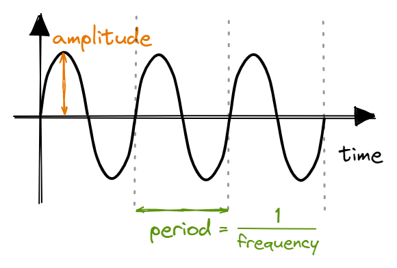
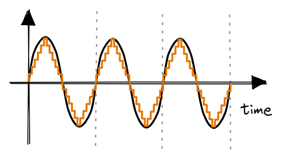
The amplitude of the wave determines the volume, while the frequency of the wave determines the pitch. Using the DAC, we discretise a sound wave and output it as a voltage wave to an audio device. The period (and hence frequency) is controlled using periodic interrupts (we’ll explore this in section 1.3).
1.3 Interrupts
Like most computing systems, an embedded system needs to perform multiple tasks concurrently. What sets an embedded system apart is its ability to use its input/output (I/O) devices to interact with the external world. The challenge under most situations is that the embedded system’s software runs much faster than its hardware. For example, it might take the software 1\(\mu\)s to ask the hardware to clear the LCD, but the hardware might take 1ms to complete the command - that is 1000 times slower! While waiting for the I/O to complete, what should the software do?
One thing the software can do is to keep checking on the status of the hardware and take an action only when the hardware sets the completion flag. This is known as a busy-wait. However, this is a very inefficient use of processor time given that the software could have completed thousands of instructions while waiting for the hardware. The alternative would be to work on other things and only take an action after being notified by the hardware of its task completion. This is known as a interrupt.
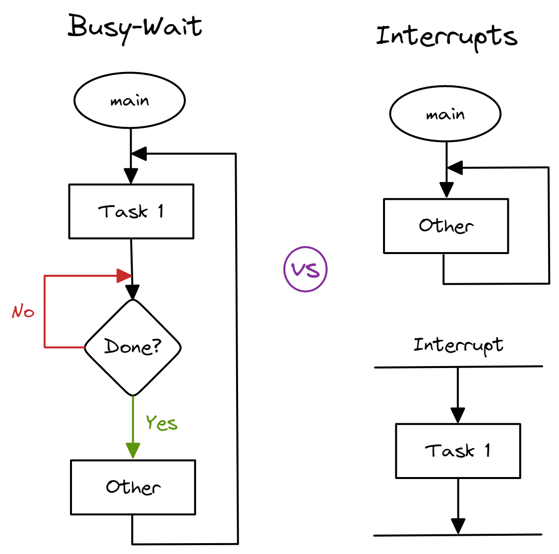
We can illustrate this difference using an analogy. Imagine that you are expecting a call from your boss. Using busy-wait is like staring at your phone waiting for it to ring, while using an interrupt is working on your other tasks and only focusing on your phone when it rings. Using busy-wait is far less efficient as you could have been working on other tasks while waiting for your phone to ring. Therefore, using interrupts enables embedded systems to make efficient use of processor time, allowing them to be truly responsive and real-time. Next, we will explore what interrupts are and how we use them.
1.3.1 What are Interrupts?
An interrupt is the automatic transfer of software execution in response to a hardware event that is asynchronous with the current software execution. This hardware event is called a trigger. A trigger can be an external event (e.g., new data is available on an input) or an internal event (e.g., periodic timer). The hardware sets the trigger flag which causes an interrupt.
When there is an interrupt, where is software execution transferred to? It is transferred to the Interrupt Service Routine (ISR). The ISR is a software module that handles the trigger, such as reading in new data available on an input. At the end, it explicitly clears the trigger flag that caused the interrupt and returns software execution.
You might then wonder, how does the system transfer software execution to the ISR? An interrupt causes a context switch that transfers software execution to the ISR:
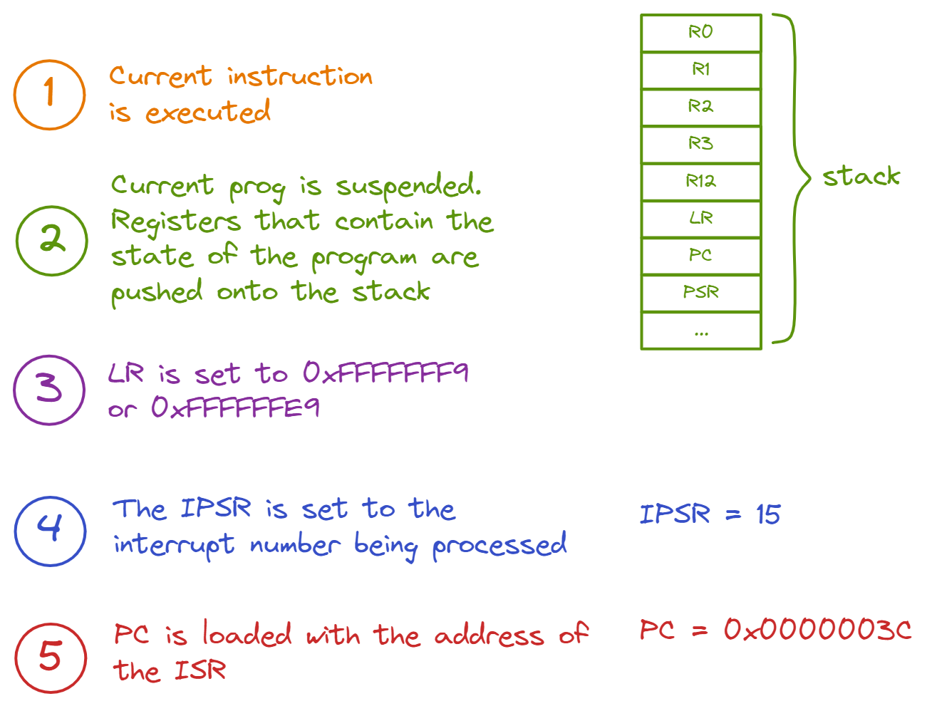
In step 2, 8 registers are pushed onto the stack. If the floating point unit is active on the EK-TM4C123GXL, an additional 18 words will be pushed onto the stack representing the floating point state. Note that LR is Link Return, IPSR is Interrupt Program Status Register and PC is Program Counter. The LR is a register that is set to a specific value signifying that an ISR is being run. It is set to 0xFFFFFFE9 if floating point registers are pushed onto the stack in step 2. The LR is used when returning from the ISR - it will pop 8 or 26 words depending on whether floating point registers are pushed onto the stack. The IPSR contains the number of the interrupt being processed (e.g., 15 is the number of the SysTick interrupt). The PC is a register that contains the address of the instruction that is currently being executed (e.g. 0x0000003C is address of the SysTick interrupt handler). More information of these core registers can be found on the ARM developer website.
1.3.2 Periodic Interrupts
How do we use interrupts in our video game console? We mostly use periodic interrupts - periodic interrupts are triggered by timers at regular intervals so that we can run a piece of code (the ISR) at these regular intervals. There are two specific timers in the EK-TM4C123GXL that we use: the SysTick timer and the Timer2 timer.
The SysTick timer is configured to trigger at 30 Hz (once every 0.033s), where the ISR reads from the ADC (player position) and switch inputs (fire missile), then updates the game state. The Timer2 timer is configured to trigger at 11 kHz (once every 0.000091s), where the ISR uses the DAC to produce game sounds.
1.4 Graphics
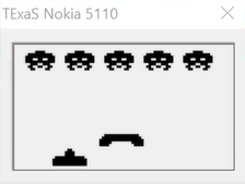
While the SysTick interrupt is used to update the game state, we also need to display graphics representing the game state. In our game, there are 4 main types of sprites: the player, the enemies, fired missiles and explosions. Given that our game is black and white, sprites can be represented as 1s (black) and 0s (white). Thus, sprites can be saved as bitmap images.
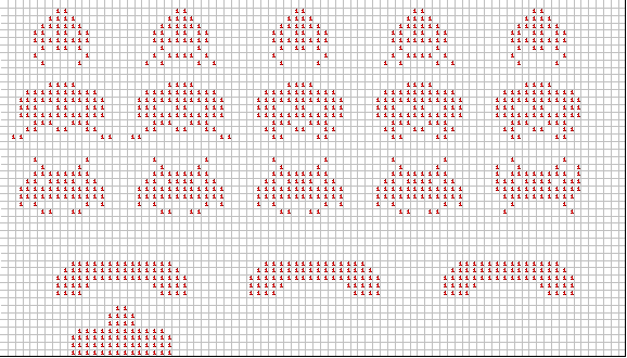
The above image is taken from the EdX course. We use a virtual Nokia5110 LCD as our display screen. The display screen is updated every time the SysTick ISR is completed at 30 Hz.
2 Bringing Everything Together
Now that we have discussed the underlying microcontroller concepts, let us integrate them together to create our video game console.
2.1 Requirements
We are to build a Space Invaders game with the following modules:
- ADC: Uses a slide potentiometer to control the x-position of the player
- Uses PE2 as analog input
- Read using 30 Hz SysTick ISR
- DAC: Play game sounds (e.g. firing missiles and explosions)
- DAC bit 0: 12 k\(\Omega\) resistor on PB0 (Least significant bit)
- DAC bit 1: 6 k\(\Omega\) resistor on PB1
- DAC bit 2: 3 k\(\Omega\) resistor on PB2
- DAC bit 3: 1.5 k\(\Omega\) resistor on PB3 (Most significant bit)
- Played using 11 kHz Timer2A ISR
- Buttons: Inputs for firing missiles
- Fire button: PE0
- Special fire button: PE1
- Read using 30 Hz SysTick ISR
- Screen: Display game state on Nokia5110 screen
- Drawn at 30 Hz
- Use USB cable to connect UART ports to virtual Nokia5110 screen (PA0 and PA1)
- Game Engine: game state updated by SysTick ISR
- Enemy sprites are slowly moved downwards
- Player sprite is moved according to the ADC
- When a missile is fired, it moves upwards towards the enemies. When it hits an enemy, the enemy is destroyed and there is an explosion.
2.2 Data Flow Graph
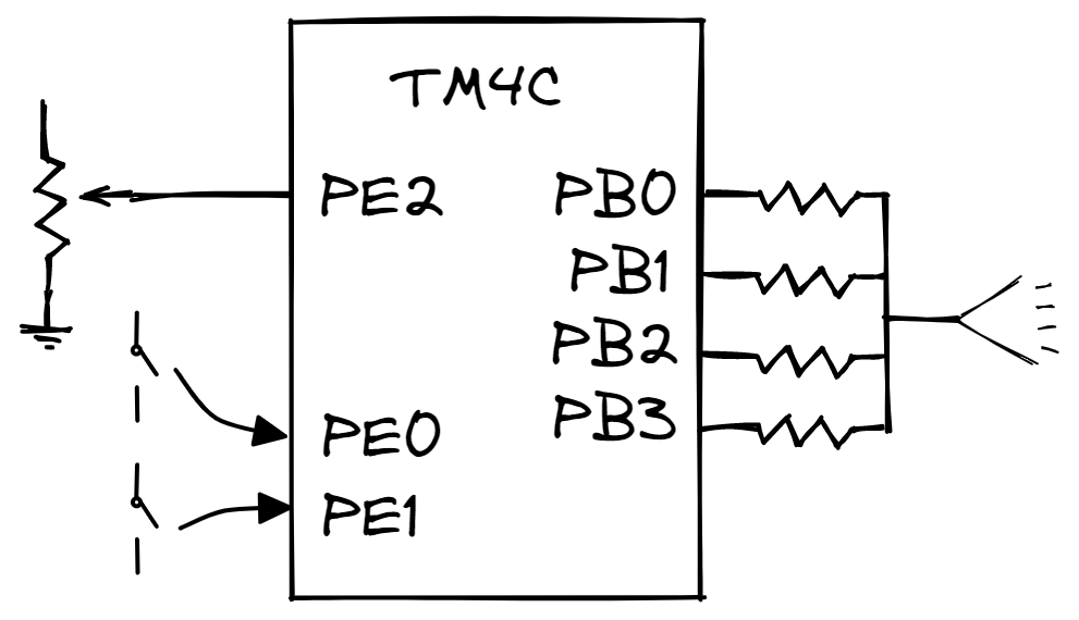
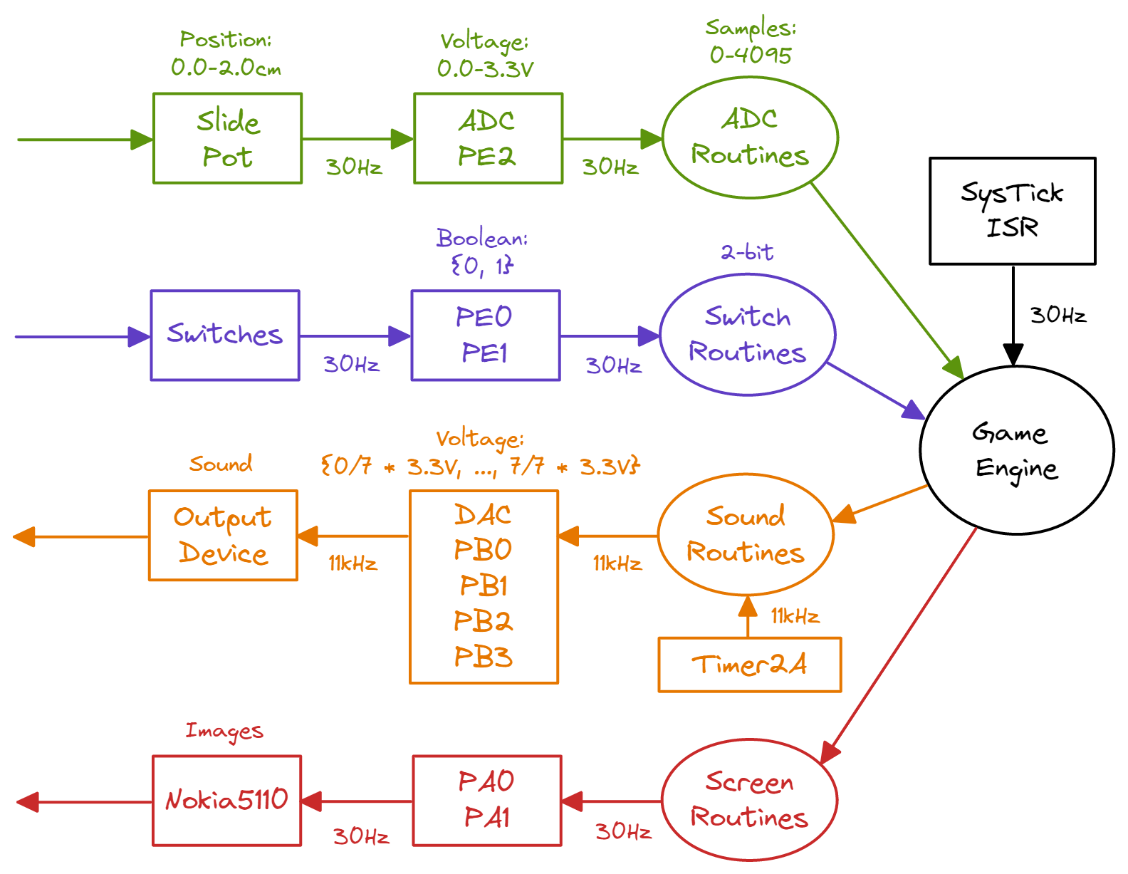
These data flow graphs show how the 5 modules of the video game console interact. We can see that there are 2 inputs (slide potentiometer and switches) and 2 outputs (sound and graphics).
2.3 Building the Electrical Circuit
Next, let’s see how we should build the electrical circuit to faciliate these 4 I/Os. First, let us build a schematic diagram:
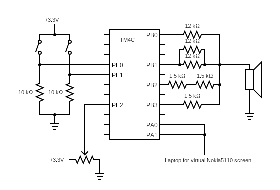
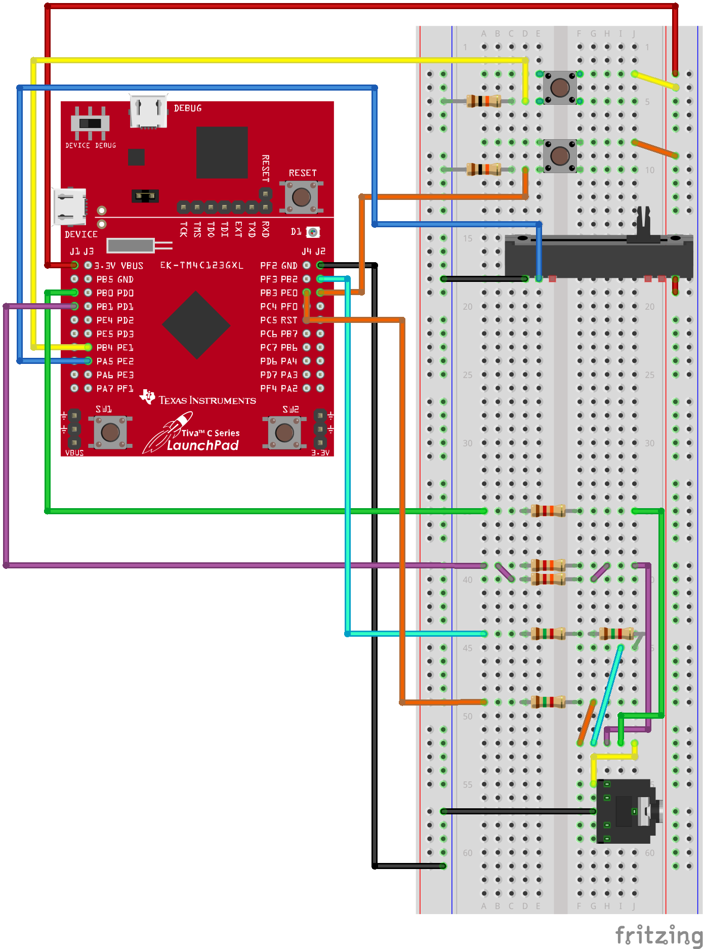
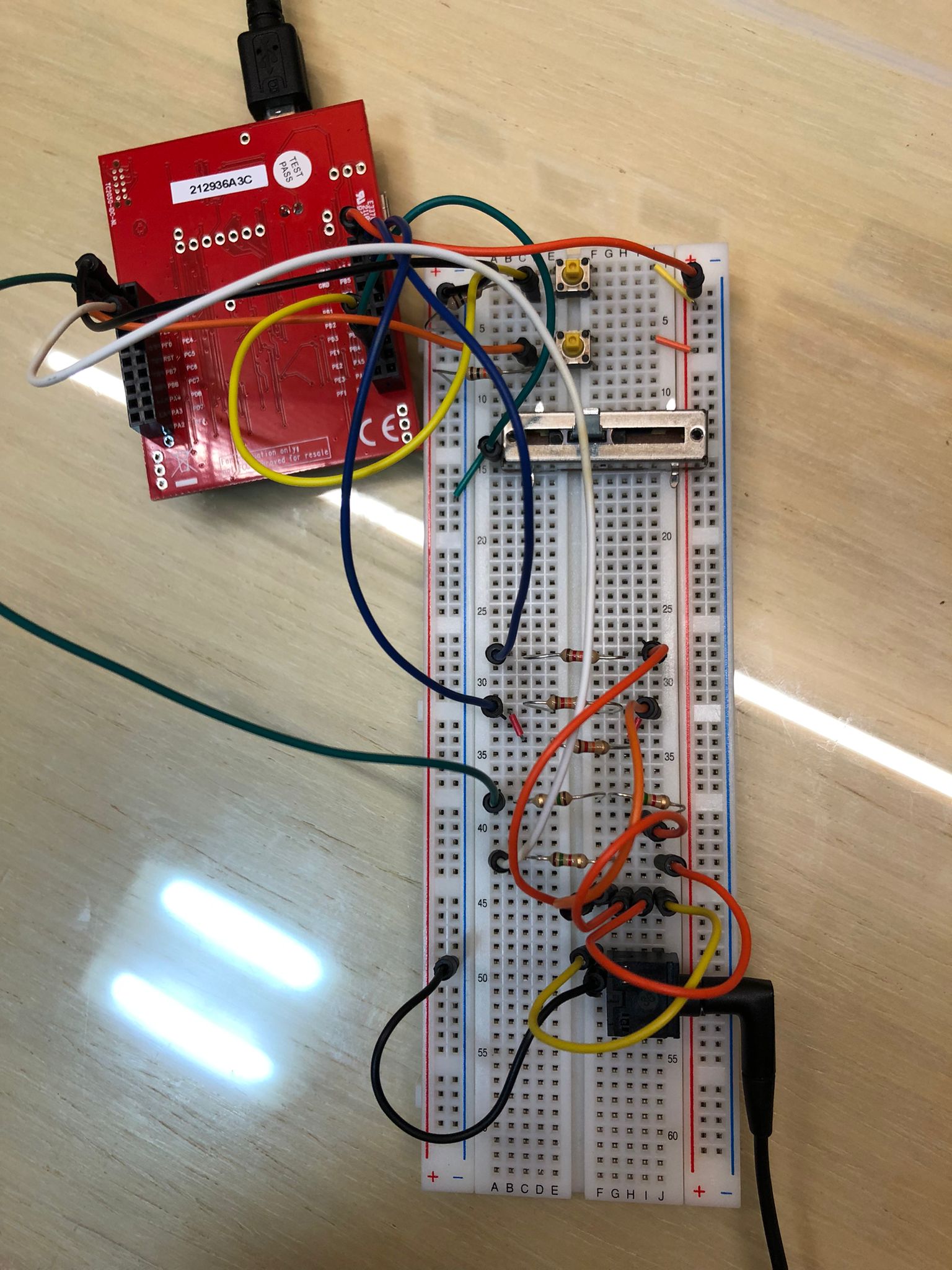
Note the 2 inputs and 1 output that are set up on the breadboard. The two switches on the top are for the switches input, while the slide potentiometer below it is the ADC input. Lastly, the resistors and audio jack at the bottom of the breadboard are for the audio output. The second output (virtual Nokia5110 screen) is connected to a laptop via a USB cable. Here’s a picture of the actual circuit:
2.4 Flow Chart
Now that we have set-up the electrical circuit, we can turn our attention to designing the software program. Here’s a flow chart depicting the general program flow:
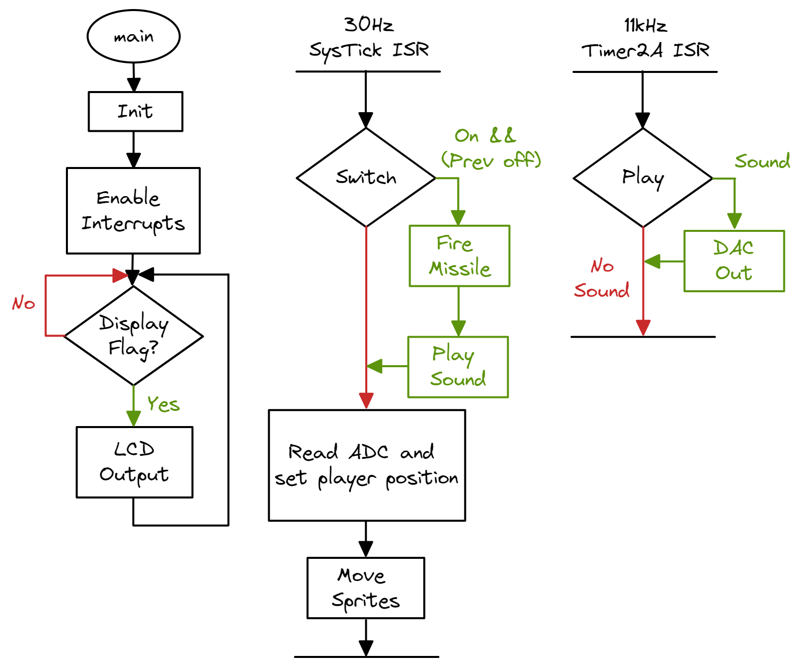
The code can be found here. Note that this is demonstrating the code I have written in SpaceInvaders.c - many other files are needed to actually run the video game console!
2.5 Demo
Here’s the final result!
As seen in the demo, when you start up the game, you will arrive at the welcome screen. After pressing the switch, you can start playing the game - aim your missile at the invaders and press fire! After destroying all the enemies, you reach the Game Over screen. Press the switch once more to transition to the welcome screen to play again. Unfortunately, there is no audio as I can only connect the audio to my headphones and not to a speaker.
3 Closing Thoughts
This project concludes the second part of the fantastic (and free!) EdX course by Professors Jonathan Valvano and Ramesh Yerraballi. I’ve learnt a lot about microcontrollers and aim to continue exploring and playing with them in the future. There are a ton of other microcontrollers like the Arduino and ESP32 that seem interesting. Stay tuned for more!